

Publication date: 2016-04-15
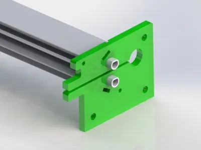
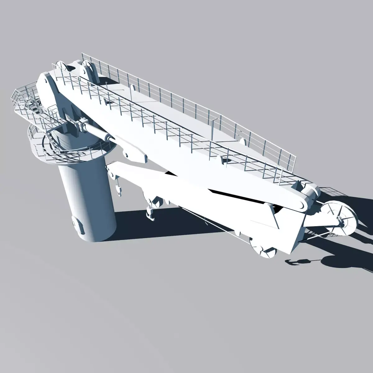
Download Peach laminator side holder Free 3D model
free
License: Royalty Free No Ai

author:
s54mtb
3D Model details
- cgtrader Platform
- Animated
- Rigged
- Ready for 3D Printing
- VR / AR / Low-poly
- PBR
- Textures
- Materials
- UV Mapping
- Polygons: 0
- Vertices: 0
- Geometry: Polygon mesh
Similar models


Find the models you need